


Blog - TECHNICAL TIPS & TRICKS - Solid State Relays - What do “dv/dt” and “di/dt” values mean ?
 “dv/dt” and “di/dt” values : what impact does the level of these values have on a Solid State Relay ?
Excessive levels of di/dt is one of the main reasons for thyristor failure. When this occurs, the stresses applied to the semiconductor devices can significantly exceed the rated values and damage the power element. In this new blog article we will explain the importance of the dv/dt and di/dt values and why they need to be considered before choosing a Solid State Relay for your application.
An overvoltage is a voltage value in excess of the normal operating voltage of a device or circuit. Depending on the level, this overvoltage can damage the components in a system.
An overcurrent is when the normal load current is exceeded. Again, depending on the value, this overcurrent can also damage the components in a system.
dv/dt is the derivative of the voltage with respect to time. In other words, it’s the change in voltage (delta V, or ΔV) divided by the change in time (delta t, or Δt), or the rate at which the voltage changes over time. The dv/dt rating is the maximum allowable rate of rise of anode to cathode voltage that will not trigger the device without any gate signal.
di/dt is the derivative of the current with respect to time. The di/dt rating is the maximum allowable rate of rise of anode to cathode current without causing any damage to the thyristor.
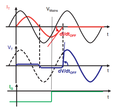
When the current across the power element (Thyristor or Triac) falls under the holding current value, the Thyristor stops conducting. With a pure resistive load this happens at the very end of the sine wave cycle, and the voltage and current are in phase. When the load has an inductive component (e.g. a motor) then there is a lag between the current and voltage. At the moment when the current drops below the holding current value, the voltage has already risen with the opposite polarity. Therefore when the triac/thyristor turns off there is a big dv/dt on it since the voltage is cut off suddenly. This situation can lead to self triggering of the triac/thyristor which can cause uncontrolled current flow.
The dv/dt rating of an SSR is an important parameter since it indicates the maximum rate of rise of anode voltage that does not bring the SSR into the conduction phase when no gate signal is applied. The dv/dt limit value is always specified in terms of voltage/microsecond.
If the rate of rise of forward anode voltage exceeds the specified maximum limit, then it causes switching from OFF state to ON state. In other words, if dv/dt increases beyond the specified value for the SSR, then it leads to false triggering of the SSR which is an undesired condition.
During the turn-ON process of the SSR, a limit on the di/dt value is always specified in terms of amperes/microsecond. Taking care to not exceed this value will allow for reliable operation of the SSR.
When di/dt is higher than the maximum value mentioned in the specifications, the anode to cathode current can rise too quickly so that the conductive area does not have enough time to spread over the entire silicon area. This then leads to the creation of hot spots near the gate connectionsince there is high current density in the junction region. The creation of hot spots can increase the junction temperature of semiconductor beyond the maximum permissible limit. As a result, the power element can suffer a permanent failure :
The di/dt limit value depends mainly on the speed of propagation and diffusion of the silicon of the thyristor/triac.
In order to keep the dv/dt values within the specified limits during the turn ON process of the SSR, an RC network can be implemented. This is also called a Snubber (or SnubberLess elements with high dv/dt withstand levels). Some of celduc’s solid state relays are fitted with SnubberLess or RC Network elements :
-Zero-cross Solid State Relays : SO8, SA/SU8, etc. These solid state relays are suitable for all types of loads
-Random or Instantaneous Solid State Relays are recommended for highly inductive loads : SO7, SU7, etc.
These products should be considered when you wish to control non-resistive loads, or when the maximum dv/dt of the triac/ thyristor may be exceeded.
On capacitive loads, when the power element closes, the di/dt value is generally critical. In this case, an inductor installed in series reduces the fast transitions, thus smoothing the current.
celduc’s SO8/SU8/SGT8 … series use specific technologies to minimize trigger voltages and synchronism to limit these sudden current variations on capacitive loads (batteries, power supply, etc.).
Maximum dv/dt and di/dt values (non-repetitive) are given by celduc in its data-sheets : above this limit, Thyristors/triacs may be damaged.

– 500 V/μs means that during every microsecond the voltage increases by 500 Volts.
– 50A/μs means that during every microsecond the current increasesby 50 Amps.
During turn-on, the maximum rate of rise of current and voltage should not exceed these maximum di/dt and dv/dt values.
“dv/dt” and “di/dt” values should be taken into account when choosing Solid State Relays, especially for non-resistive loads. Celduc offers Solid State Relays fitted with SnubberLess or RC Network elements, which help keep “dv/dt” and “di/dt” levels within the specified limits.
![]()
D‑U‑N‑S® Number : 117690071
Phone : 312-420-0519
434 E. Main Street, #429
Centerport NY 11721
USA

