


Blog - NOS MARCHÉS - SSR for Semiconductors and Components
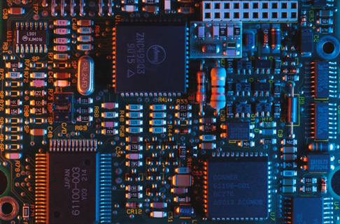 Semiconductors and Components are important to Modern Living as they power almost everything in our daily lives. From smartphones to cars, semiconductors evolved to improve technologies. Semiconductors are the brains of modern electronics. As a result, the global semiconductor market is growing almost continuously from the start of the 21st century. In the first quarter of 2021, it was estimated to 101 billion €uros.
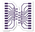
An electronic component is an element intended to be assembled with others in order to perform one or more electronic functions. They are ubiquitous in all electronic objects. The value of the global electronic components market increased from 250 billion €uros in 2012 to 350 billion €uros in 2019.
Currently, these markets are suffering a big shortage: demand is growing exponentially and the industry is unable to meet it.
Celduc relais has an extensive experience serving the Electronics industry, let’s go into more details with some case studies.
For all equipment used for these processes Solid State Relays are widely used because of their ability to work in harsh environments without operating problems
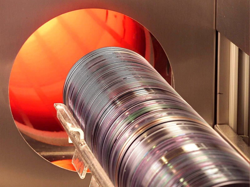 Semiconductor annealing (heat treatment) is used for activating silicon wafers injected with impurities (increasing density/speed). The temperature should be accurate at this stage. In fact, if the heat penetrates too deeply, the impurities will diffuse into deeper layers, forming a thick semiconductor layer. Flash annealing limits heat treatment to the surface layer, preventing the diffusion of impurities and allowing the production of extremely thin semiconductor layers.
During diffusion process dopants are introduced inside the material. Oxidation process forces oxygen, vapour, to diffuse into the wafer surface at high temperatures between 800 and 1200°C so that a thin, smooth layer of silicon dioxide can be created.
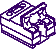
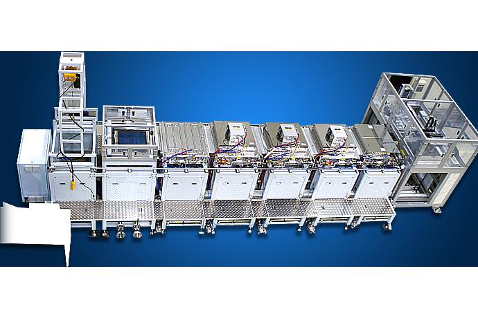
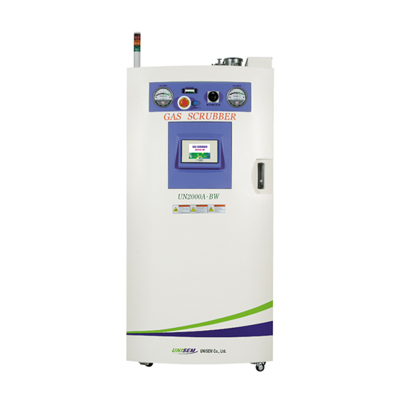 Scrubber systems are designed to perform one of the most important process functions in Integrated Circuit manufacturing : wafer cleaning. It can be used between any two steps in the wafer manufacturing process. These systems remove contaminants such as particles, residues and other unwanted surface defects that can cause fatal errors in IC devices.es machines de récurage sont conçues pour exécuter l’une des fonctions les plus importantes dans le process de fabrication de semi-conducteurs : le nettoyage des “wafers”. Ces systèmes éliminent les particules contaminantes telles que les résidus ou autres défauts de surface indésirables. Nos relais statiques sont indispensables pour le contrôle des éléments chauffants.
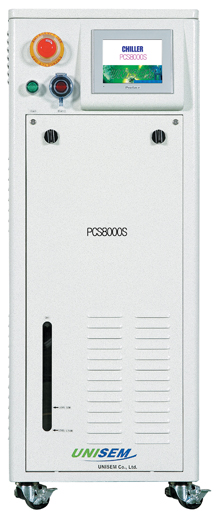 This sensitive process requires accuracy when dealing with liquid cooling or air conditioning cooling.
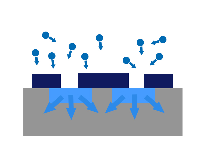
 Dry etching is to remove layers from the surface of a wafer during the manufacturing process. Plasmas or etchant gases are used to remove the substrate material.
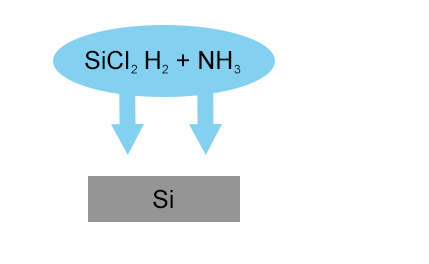
 Chemical vapour deposition, or CVD, is a commonly used method of creating thin films used in semiconductor manufacturing. The coating material is vaporized inside a vacuum chamber and begins to uniformly settle on the substrate.
Gases have been a key enabler of the electronics industry. At almost all stages of semiconductors manufacturing, gases are used : Deposition, Photolithography, Etching, Doping, Annealing, Chamber cleaning…
These systems are used to safely supply special gases required for semiconductor and solar manufacturing processes.
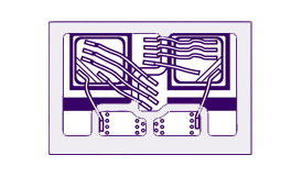
This technology is used to solder the electronic components on a PCB. This technology is used to solder the electronic components on a PCB. This reliable and automatic system is widely used in the electronics industry. Wave soldering process is composed by four steps:
SSRs are widely used at steps 2 and 3 of the manufacturing process. They switch on & off the heater to keep the temperature stable and to allow a better soldering.
In this equipment we recommend the use of Analogue Controllers : Phase angle controllers allow the load power to be finely adjusted.
Reflow soldering is another process to sold components on PCB. Here are the differents steps in the process:
SSRs are widely used at the steps 3 and 4 of the manufacturing process. SSR control of the heating zones will ensure that temperature requirements are accurately carried out.
The celduc® group specializes in electrical engineering and power electronics and has turned to markets and customers all over the world. Founded in 1964 by Michel GUICHARD and located near Saint-Etienne, celduc® is the only French company to have solid state switching technology.
celduc® relais controls the entire chain: study, design, manufacture, testing and marketing. celduc® relais manufactures not only the widest range in the field of solid-state relays, but also its main strategic production and control equipment in terms of knowledge and technical expertise. Thanks to this powerful and unique tool, celduc® relais products are present all over the world, and bear the imprint of the largest industrial groups.
If you need our support for new projects, contact our team of experts
![]()
D‑U‑N‑S® Number : 382274546
Sales department France :
+33 (0) 4 77 53 90 20
Export sales department :
+33 (0) 4 77 53 90 21
———————————-
Gender Equality Index 2026
Based on 2025 data
Final result: 88/100 (for more information)

